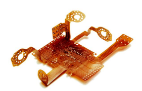
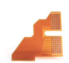
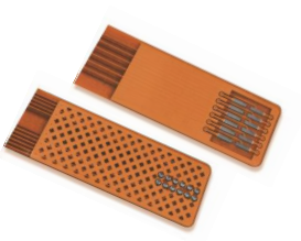
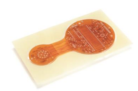
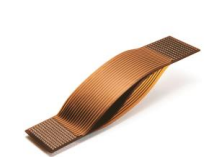
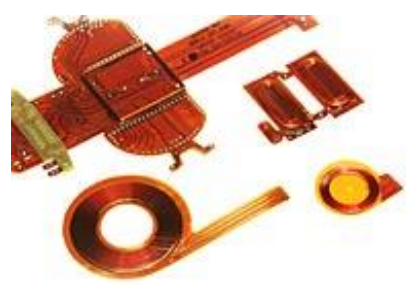
Types of Flex Circuits
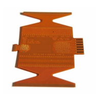
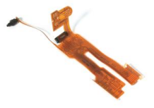
- Flex: Flexible version of a Printed Circuit Board (PCB), with unique capabilities. Flex circuits offer the same advantages of a printed circuit board: repeatability, reliability, and high density but with the added “twist” of flexibility and vibration resistance. The most important attribute compelling designers to adopt flex circuit technology is the capability of the flex circuit to assume three-dimensional configurations.
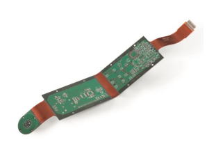
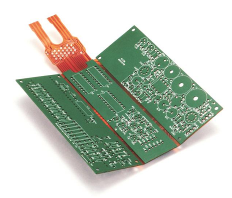
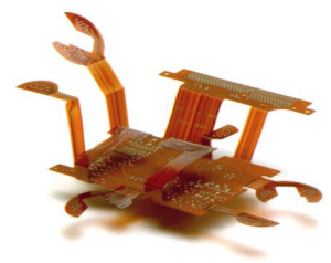
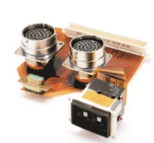
- Rigid-flex: A blend of rigid and flex emphasizing the best of both constructions, adding synergistic capabilities neither possess alone. In its most typical configuration, the rigid-flex is a series of rigid PCBs joined by integrated flex circuits (with emphasis on the high percentage of rigid area content). Circuits designed primarily as flex circuits have great opportunities to increase your design capabilities when integrated rigid areas are added. Rigid areas provide excellent hard mount points for components, connectors, and chassis while flex areas offer dynamic flexing, flex to fit, and component mounting poised to take advantage of these low mass and vibration resistant zones. This blending leads to creative solutions for your most demanding applications
- High Density Interconnect (HDI): High Density Interconnect (HDI) flexible circuits offer increased design, layout and construction options over typical flexible circuits. Each High Density Interconnect incorporates microvias and fine features to achieve highly dense flex circuitry, smaller form factor and increased functionality. This technology offers better electrical performance, access to advanced integrated circuit (IC) package use, and improved reliability through the use of microvias and thinner materials.
Benefits of Flex Circuits
High reliability
Repeatable installation
Compared to discrete wiring, or ribbon cable, a flex circuit offers a customized repeatable routing path within your assembly. This gives you dependability where you need it. The longevity of a flex circuit can reduce service calls.
Harsh environments
Standard practice for flex boards is to cover the conductors with polyimide. This dielectric layer protects your circuits far beyond the capability of simple solder mask. Other base and cover materials are available for a broad range of ambient conditions.
Long duty cycles
By design, a flex circuit can be made very thin, yet robust enough to withstand thousands to millions of flexing cycles while carrying signal and power without a break.
High vibration
Under vibration and/or high acceleration, a flex circuit’s ductility and low mass will reduce the impact upon itself and solder joints. By contrast, a PCB’s higher vibrational mass will increase stresses upon itself, components and solder joints.
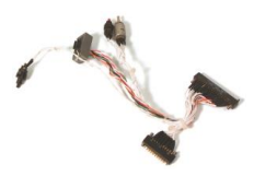
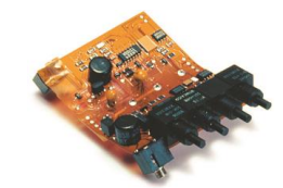
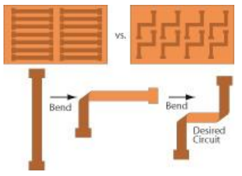
Before: A tangle of wires connects four circuit boards.
The flex circuit solution: A single circuit with 7 stiffeners and 2 connectors provides all the needed interconnects.
After: The package is neat, lightweight, and less susceptible to connection failure.
Superior packaging options
Flex circuits can be shaped to fit where no other design can. They are a hybrid of ordinary printed circuit boards and round wire, exhibiting benefits of each. In essence, flex circuits give you unlimited freedom of packaging geometry while retaining the precision density and repeatability of printed circuits.
Flex vs. wiring harness
- Space and weight reduction: A single flex circuit can replace several hardboards, cables, and connectors.
- Fast assembly: Flex circuits eliminate the need to color code and wrap bundles of wire, reducing the chance of assembly rejects and in-service failures. Total installed costs are lower, especially with volume production.
- Repeatable wire routing: Eliminate wire routing errors; reducing test time, rework, and rejects.
- Robust connections: Flat foil conductors dissipate heat better, carrying more current than round wires of the same cross-sectional area. Conductor patterns in a flex circuit maintain uniform electrical characteristics. Noise, crosstalk, and impedance can be predicted and controlled.
Flex vs. Rigid board (PCB)
- Versatile shape: The most important attribute compelling designers to adopt flex circuit technology is the capability of the flex circuit to assume threedimensional configurations.
- Lower mass: With a little experimentation and imagination, a flex circuit can save up to 75% of the space and/or weight of conventional wiring.
- Vibration resistance: Recurring costs are lower than many wire harnesses, and since a flex circuit is more resistant to shock and vibrations than a PCB, repair and replacement costs are less.
- Component mounting: Surface mount component mounting on flex is achievable using selectively bonded stiffeners where required.
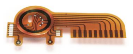
Rigid-flex
- Double side component mounting: Rigid-flex circuits are the ideal solution for flex circuits where surface mount components must be mounted on both sides of the board.
- Total cost of ownership: The maximum benefit of rigid-flex is realized when the complete installation is reviewed for total cost of ownership. Using rigid-flex eliminates connections in the flex-to-rigid transitions which can improve reliability and improve impedance control.
- Most capable/Maximum vibration resistance: Lets you integrate the best capabilities of resistant rigid areas and resilient flex areas.
- High mass component mounting: When mounting a high mass component, a rigid board is the right solution. A rigid-flex board gives you a smooth transition between rigid and flex areas while preserving the benefits of each.
Design Options
Rigid-flex
Hybrid hardboard/flex circuits can have up to sixteen layers. They replace bulky wire harnesses with a compact, robust design.
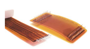
Pins
We can braze or solder pins to circuits, either through-holes or as extensions to conductors.
Fine lines
0.002″ conductors and spaces are possible.
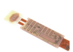
Stiffeners
An inexpensive alternative to rigid-flex.
Connectors
Built-in connectors speed your assembly. Optional epoxy potting creates a seal between the circuit and connector.
Shielding
Solid or patterned shield planes reduce noise and control impedance of signal lines. Use matched impedance flex circuits for high-speed signal integrity.
Assembly
pallet Stiffener material frames the circuit to hold it flat during assembly operations. After soldering or component placement, just clip out and install.
Factory forming
Factory formed circuits follow tight curves to save space.

Coils
unique flat wound inductive coils can be laminated into flex circuits. Applications include pacemaker antennas and eddy current generators.
Surface mount
Combine the space and weight savings of surface mounting with those of flex circuits for the ultimate in high-density packaging.
Selective bonding
For better flexibility along circuit arms, individual layers are unbonded and allowed to flex freely. Each layer has its own substrate and cover.
Design Guidelines
Specification documents:
Consult standard specifications and design documents pertaining to your application and circuit requirements.
IPC specifications
- IPC-2221A, Generic Standard on Printed Board Design
- IPC-2223, Sectional Design Standard for Flexible Printed Boards.
- IPC-4101, Specification for Base Materials for Rigid and Multilayer Printed Boards
- IPC-4202, Flexible Base Dielectrics for Use in Flexible Printed Circuitry
- IPC-4203, Adhesive Coated Dielectric Films for Use as Cover Sheets for Flexible Printed Circuitry and Flexible Adhesive Bonding Films
- IPC-4204 Flexible Metal-Clad Dielectrics for Use in Fabrication of Flexible Printed Circuitry
- IPC-6013, Qualification and Performance Specification for Flexible Printed Wiring
- IPC-MF-4562, Copper Foil for Printed Wiring Applications
- IPC Position Paper: Transitioning from MIL-P50884C and MIL-PRF-31032 to IPC-6013 and Amendment 1
Military
- MIL-P-50884 (inactive for new designs), Printed Wiring, Flexible and Rigid-flex for Electronic Printed Wiring
- MIL-PRF-31032/3A, Printed Wiring Board, Flexible, Single and Double Layer, With or Without Plated Holes, With or Without Stiffeners, for Soldered Part Mounting
- MIL-PRF-31032/4A, Printed Wiring Board, RigidFlex or Flexible, Multilayer, with Plated Holes, with or Without Stiffeners, for Soldered Part Mounting
IPC recommends that companies using MIL-PRF31032 specifications for printed circuits alternatively specify that flexible circuits be supplied under IPC-6013 Class 3 performance requirements. Government agencies have generally accepted that this is a COTS (Commercial, Off-The-Shelf) equivalent to MIL-PRF31032. If your circuit must meet performance requirements of MIL-P-50884, MIL-PRF-31032 or IPC6013; we urge you to read the IPC-2223 design specification for flexible circuits and follow its recommendations.
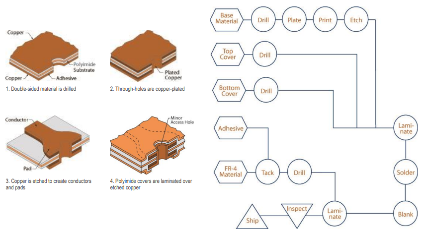
Manufacturing a flex circuit
Building a flex circuit generally involves the same steps from circuit to circuit. However, certain circuit designs can add cost. The flow chart and illustrations identify some cost driven issues, such as access holes, plated throughholes, etc. The flow chart shows the manufacturing process for a standard double-layer circuit with a stiffener.
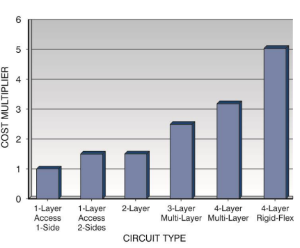
Cost impact of layer count
The information for the chart was taken from a sample of circuits built with standard materials. This chart is not intended to be used as a price guide. However, it does show that circuit cost generally rises with layer count.
It is in your best interest to consider all options to minimize cost. For example, use two circuits to do the job of one. Two double-layer circuits may be less expensive than one four-layer circuit. But the cost savings of the circuit may be offset by additional assembly requirements. Circuits can also be folded in order to save space and layers. Each situation is unique. A relatively small amount of time invested in project assessment can result in significant savings overall.
Standard Design Recommendations
Design differences and special considerations
Define circuit parameters by application
It may be helpful to use a paper template to represent the circuit. Experiment with bending and forming the template to optimize shape and fit. When designing the final shape, consider how the circuits will lay out on a processing panel (“nesting”). The greater the number of circuits per panel, the lower the cost.
Another consideration concerns rigid-flex. While we are capable of building a traditional rigid-flex board for you, it may not be your best choice. Multilayer or stiffened flex boards may be able to meet your requirements for component and board mounting at reduced cost.
Flex circuit vs. hardboards
Designing a flex circuit is only one step away from designing a hardboard. The most important design difference to keep in mind is the three-dimensionality of a flex circuit. Creative bending and flexing can save space and layers. Other important differences:
- Flex circuits both require and permit looser tolerances than hardboards.
- Because arms can flex, design them slightly longer than required.
Design tips to minimize circuit cost
- Consider how circuits will be “nested” on a panel.
- Keep circuits small; consider using a set of smaller circuits instead of one large circuit.
- Follow recommended tolerances whenever possible.
- Design unbonded areas only where they are absolutely necessary.
- If circuits have only a few layers, using stiffeners can be far less expensive than a rigid-flex circuit.
Special considerations for rigid-flex
- Rigid-flex is the ideal solution for applications with multiple rigid PCBs having SMT components on both sides and requiring interconnects between the rigid PCBs.
- Before designing a rigid-flex circuit, make certain that it is truly what you need. If the circuit only has a few layers, stiffeners are a less expensive alternative to rigid-flex.
- It is most cost effective to build a rigid-flex with an even number of layers. All rigid portions of the circuit should have the same number and stack-up of layers.
- Observe aspect ratio (hole depth/hole diameter) limits.
- we build circuits up to 20 layers, but costs increase significantly above 10 layers.
- Expect a trim tolerance similar to that of a steel rule die from hole-to-border and border-to-border.
- Hole positional tolerance within a cluster of holes is generally +/-.003”. Add .002” per inch for tolerances between cluster datums, especially those in different rigid areas.
- Minimum inside corner radius of 0.031″ (0.79mm) is standard, but smaller radii are possible.
- Unbonded layers can increase flexibility in multilayer flex circuits, but this option is more expensive. Specify unbonded layers only in areas of the circuit that will bend.
- we can provide an epoxy fillet on stiffener edges that will bend or flex.
- For rigid-flex circuits, it is less expensive to have plated through-holes in the rigid portions only.
- we can provide blind and buried vias in rigid-flex circuits.
How to improve flexibility and bend radius
Two or more layer circuits are best suited to static applications, which flexes only during installation.
Several problems can arise when a circuit is bent sharply. Compression can cause wrinkles in the cover coat on the inside of the bend. Stretching can result in tears in the cover material and/or broken conductors on the outside of the bend.
Start the mechanical design by establishing the bend radius. If the radius is at least ten times the thickness of the material, there is a good chance that the circuit will function reliably.
The minimum allowable bend radius depends on a number of factors, and is best defined by IPC-2223. Overall circuit thickness is slightly less than the sum of the individual insulator, adhesive and foils layer thicknesses.
Bend radius (flexibility):
Double-layer: 12 × circuit thickness (minimum)
Multilayer: 24 × circuit thickness (minimum)
Circuit thickness is approximately 0.006″ (0.150mm) per layer.
Incorporate these features into multilayer and reduced bend ratio designs to increase reliability
- Reduce overall thickness in the flex area
- Reduce the base copper weight (and the corresponding adhesive thicknesses) or reduce the dielectric thickness.
- Use adhesiveless base materials. Adhesiveless materials will usually reduce the starting thickness of each substrate by 1-2 mils (25-50μm) when compared to adhesive based substrates.
- Eliminate copper plating on the conductors in the flex area by utilizing selective (pads-only) plating or adding outer pads-only layers to the circuit.
2. Make the circuit robust to withstand flexing.
- Balance the conductor weights and material thicknesses on each side of the neutral bend axis.
- To increase flexibility, conductors should be staggered from layer to layer and not stacked on top of each other.
- Conductors should always be routed as close to perpendicular as possible through bend areas.
- Conductor thickness and width should remain constant in bend areas.
- Add stiffeners under termination areas to remove the stresses around the terminations. Consider strain relief at the edges of the stiffeners.
- Plated through-holes should be kept out of the bend areas.
- If the circuit will be bent within 1″ (25.4mm) of termination pads, fillets should be placed at each conductor/pad interface. Stresses from a bend are not isolated to the immediate bend area and residual stresses can radiate out from the bend.
- If shields and/or ground planes are required on the circuit, use a cross-hatched pattern rather than solid copper. Another shielding option is a screened-on conductive coating such as silver epoxy, which is much more flexible than copper
- Incorporate tear stops or reliefs for slits in the circuit. The end of the slit represents a vulnerable point for a tear to start and to propagate.
- Avoid any discontinuities in the cover coat or substrate near a bend.

- The circuit outline should be designed so there are no twists in the finished assembly. Any burr or irregularity from the blanking operation could potentially propagate into a tear.
- Consider factory forming. Reliable bend radii tighter than 10:1 are possible if the circuit is formed using specialized tooling and will only be flexed one time.
- If bend reliability is still a concern, consider “unbonding” the flexible substrates from each other. Since each of the substrates in the unbonded area has a much lower thickness than the total circuit, they are able to bend tighter than if they were fully bonded.
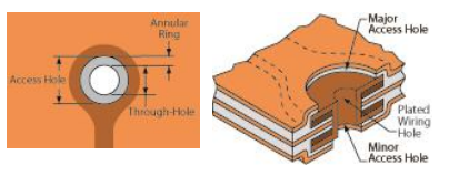
HolesPreferred minimum design requirements for pad and access hole sizing for IPC class 3 circuits*
| Feature | Design pad size | Design Cover size |
| Type 1+5 circuits | 0.024″ (0.61mm) + T | 0.030″ (0.76mm) + t |
| Outside pads-Types 2-4 | 0.018″ (0.48mm) + T | 0.022″ (0.56mm) + t |
| nterior pads-Types 2-4 | 0.014″ (0.36mm) + T | NA |
t = nominal through-hole diameter.
Pad and major access hole design requirements are based on typical IPC annular ring requirements of 0.002″ (0.05mm) minimum for all external layers for types 2-4, and 0.001″ (0.025mm) minimum for multilayer inner layers.
Vias
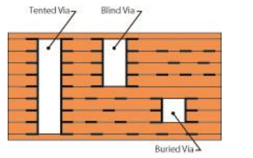
We can provide circuits with covers that have no access holes exposing the vias (called “tented vias”). We can also provide blind and buried vias in multilayer and rigid-flex circuits. Blind vias connect the top or bottom conductor layer to adjoining layers, but the via does not extend through all layers. A buried via only connects internal layers and is not exposed in the finished circuit. Blind and buried vias increase circuit cost, but they free up space for additional conductors on the non-drilled layers. We can also planerize blind vias in surface mount pads for additional space savings
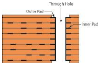
Through-hole (Thruhole)
Plated through-holes (PTH) connect together the top, bottom, and any required internal conductor layers. PTHs are drilled oversize to accommodate the thickness of the copper plating that will cover the entire barrel of the hole as well as the surface of the outer pads. Exterior pads may be plated along with the entire foil surface or selectively plated just at the PTH site.
Stiffener holes:
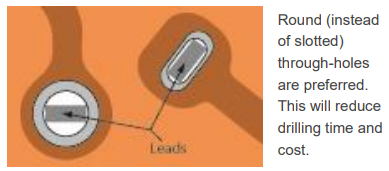
Stiffener holes should be a minimum of 0.015″ (0.38mm) in diameter larger than the access hole. It is better if the access hole underneath the stiffener hole is a minor access hole in order to increase the stiffener web between holes and to prevent potential solder wicking between the stiffener and the circuit. The customer must allow tangency. Round stiffener holes are less expensive than slotted stiffener holes, and thinner stiffener material (less than 0.031″/0.79mm) is less expensive to process.
Wiring holes
We can drill through-holes as small as 0.0039″ (0.10mm). A 0.020″ (0.50mm) through-hole size is typical. Standard finished hole tolerance is ±0.003″ (0.08mm). For all circuits, the finished through-hole size should be 0.003″ (0.08mm) to 0.010″ (0.25mm) larger in diameter than the component lead. This depends on the number of leads per component, and the positional tolerance of the component leads.
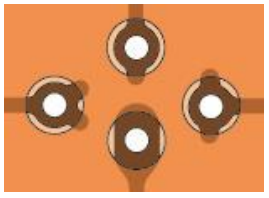
Pads
Whenever possible, design pads larger than the access holes as this allows for a more rugged connection. If space is critical, use hold-down tabs. A variety of holddown tab designs are available.
Pad fillets
Pad fillets improve etched yield and material strength. Fillets are appropriate when the pad diameter is greater than the connecting strand width. Acute angles at the interface between conductors and pads are to be avoided by using fillets to minimize the concentration of stress at the interface.
Surface mount access
We can provide flex circuits with areas that are specifically designed for surface mount components. Because covers are drilled (not silk-screened), round access holes are easier to provide. Square access holes will add to cost because the pad access area would have to be punched out with a punch-and-die. Square pads with round access holes are a good compromise. Below are some ideas for configuring pads for surface mount.

Liquid Photo Imageable coverlay materials are also available, and can provide intricate, irregular shaped openings for dense surface mount patterns.
Soldering tips
- Since polyimide absorbs moisture, circuits must be baked (1 hour @ 120°C minimum) before soldering.
- Pads located in large conductor areas, such as ground planes, voltage planes, or heat sinks, should be provided with relief areas, as illustrated. This limits heat dissipation for easier soldering.
- When hand soldering pins in dense clusters, avoid soldering adjacent pins one after another. Move around to avoid local overheating.
- We can solder connectors or components (SMT or Through-hole) as an added service.
- We can supply circuits in panel form for easier component assembly

Tolerances
You are not limited to the tolerances listed in this section. Tighter tolerances are achievable, but often at a higher cost. Accordingly, more relaxed tolerances will typically cost less. Even with relaxed tolerances, a flex circuit will have a uniformity that is impossible to attain with conventional wiring. The flexibility of materials within a flex circuit construction allow it to be more compliant than rigid circuits, so it is not always necessary to specify tight tolerances across all dimensions.
Trimming
Each trimming method has advantages and disadvantages. Routing and laser trimming provide hard tooling (punch and die) tolerances for small quantities of circuits. Laser trimming is also capable of creating complex cutouts not feasible with other methods. Steel rule dies (SRD) are best for intermediate quantities and tolerances. Chemical milled dies (CMD) offer tighter tolerances than SRDs for an incremental increase in cost. Hard tooling (punch and die) is recommended for tight tolerances, complex circuits, and/or high quantity. For more specific information on SRD, CMD, and punch-and-dies, see the Glossary at the end of this guide.
| Circuit dimension in inches(mm)† | Outline dimensions (profile tolerance) | Hole-to-border dimensions | Cluster to cluster§ | ||||
| SRD | CMD | Punch and die /laser | SRD | CMD | Punch and die /laser | ||
| 1 | ±0.015 (0.38) | ±0.010 (0.25) | ±0.003 (0.08) | ±0.015 (0.38) | ±0.010 (0.25) | ±0.007 (0.18) | ±0.003 (0.08) |
| 5 | ±0.020 (0.50) | ±0.015 (0.38) | ±0.007 (0.18) | ±0.020 (0.50) | ±0.015 (0.38) | ±0.012 (0.30) | ±0.007 (0.18) |
| 10 | ±0.025 (0.63) | ±0.020 (0.50) | ±0.012 (0.30) | ±0.025 (0.63) | ±0.020 (0.50) | ±0.017 (0.43) | ±0.012 (0.30) |
| 15 | ±0.030 (0.76) | ±0.025 (0.63) | ±0.017 (0.43) | ±0.030 (0.76) | ±0.025 (0.63) | ±0.022 (0.55) | ±0.017 (0.43) |
| 20 | ±0.035 (0.88) | ±0.030 (0.76) | ±0.022 (0.55) | ±0.035 (0.88) | ±0.030 (0.76) | ±0.027 (0.69) | ±0.022 (0.55) |
† Round up circuit dimension to next highest increment.
§ Represents from a group of holes to a group of holes. Holes within a group will have a tolerance of ±0.003″ (0.08mm).
Note: Dimensional tolerances are given in inches. See Glossary for definition of profile tolerance.
Solder thickness
We follows IPC-6013 requirements of coverage and solderability for solder coatings. Conductor width, thickness, and spacing we can provide a 0.004″ (0.10mm) minimum conductor width/spacing (0.0025″/0.063mm minimum at higher cost) on 1 oz. (25μm) copper and 0.005″ (0.13mm) minimum conductor width/spacing on 2 oz. (50μm) copper (for thicker copper, consult us). For best producibility, design circuit conductors at least five times wider than they are thick.
Tolerances for conductor width depend on whether the copper is plated or unplated.
| Copper thickness | Plated copper | Unplated copper |
| ½ oz. | ±0.001″ (25μm) | ±0.0005″ (25μm) |
| 1 oz. | ±0.002″ (50μm) | ±0.001″ (25μm) |
| 2 oz. | ±0.003″ (75μm) | ±0.002″ (50μm) |
| 3 oz | ±0.004″ (100μm) | ±0.003″ (75μm) |